- 您现在的位置:买卖IC网 > Sheet目录325 > FAN5701UMP30X (Fairchild Semiconductor)IC LED DVR MULTI 30MA 16-UMLP
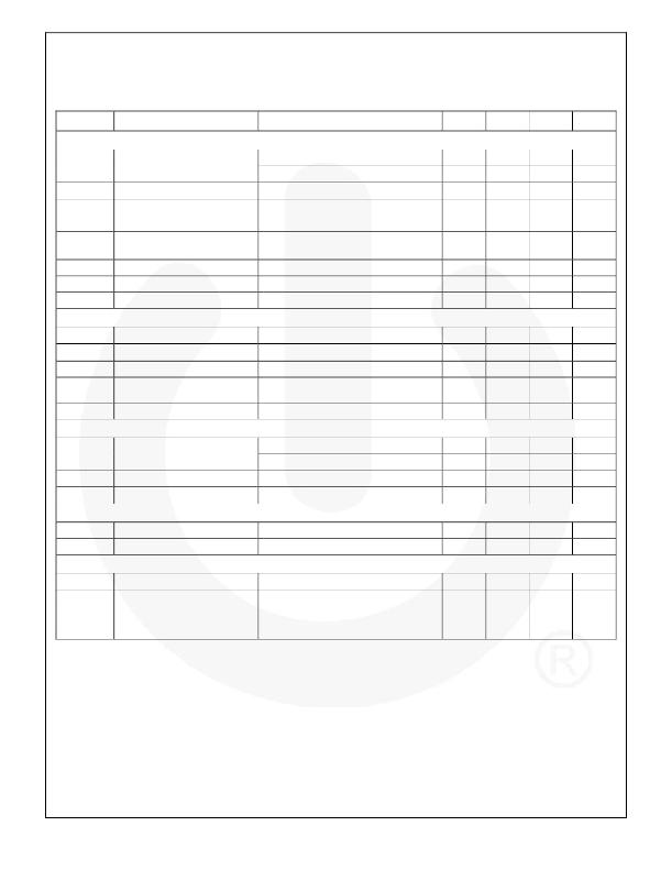
Electrical Specifications
Unless otherwise specified; V IN = 2.7V to 5.5V, T A = -40 ? C to +85 ? C, and EN = V IN . Typical values are V IN = 3.6V, T A = 25 ? C,
I LED = 20mA, and LED cathode terminals = 0.4V. Circuit and components are according to Figure 1.
Symbol
Parameter
Conditions
Min.
Typ.
Max.
Units
Power Supplies and Thermal Protection
I Q
Quiescent Supply Current
1.5x Mode, No LEDs
1x Mode, No LEDs
4.4
0.7
mA
mA
I SD
Shutdown Supply Current
EN = 0, V IN = 4.5V, T A =-40 ? C to +85 ? C
1.5
4.0
? A
V UVLO
Under-Voltage Lockout
Threshold
V IN Rising
V IN Falling
2.20
2.55
2.40
2.70
V ?
V UVHYST
OVP
T LIMIT
T HYST
Under-Voltage Lockout
Hysteresis
Over-Voltage Protection
Thermal Shutdown
Thermal Shutdown Hysteresis
150
6
150
20
mV
V
°C
°C
LED Current Sinks
I LED
I LED(MAX)
I LED_MATCH
V DTH
V HR
Absolute Current Accuracy
(3)
Maximum Diode Current
LED Current Matching (4)
1x to 1.5x Gain Transition
Threshold
Current Sink Headroom (5)
V CATHODE =0.4V, See Options for I SET
I LED = I SET
V CATHODE =0.4V, I LED = I SET
LED Cathode Voltage Falling
I LED = 90% I LED(NOMINAL)
– 10%
I SET
30
0.4
100
65
+10%
3.0
mA ?
mA ?
%
mV
mV
Charge Pump
R OUT
Output Resistance
1.5x Mode
1x Mode
2.4
0.9
Ω
Ω
f SW
t START
Switching Frequency
Startup Time
V OUT = 90% of Steady State
0.9
1.2
250
1.5
MHz
? s ?
PWM Dimming
f PWM
PWM Dimming Frequency
t ON_LED = 15μs (Minimum)
20
kHz
D PWM
PWM Duty-Cycle
f PWM = 100Hz
0.15
100.00
%
Logic Inputs (EN, PWMA, PWMB)
V IH
V IL
HIGH-Level Input Voltage
LOW-Level Input Voltage
1.2
0.4
V
V
V IMAX
Maximum Input Voltage
1.8
5.5
V ?
I IN
Input Bias Current
Input Tied to GND or V IN
0.01
1.00
? A
Notes:
3.
4.
5.
The maximum total output current for the IC should be limited to 180mA. The total output current can be split between the
two groups (IDxA = IDxB = 30mA maximum). Under maximum output current conditions, special attention must be given
to input voltage and LED forward voltage to ensure proper current regulation. See the Maximum Output Current section of
the datasheet for more information .
For the two groups of current sinks on a part (GroupA and GroupB), the following are determined: the maximum sink
current in the group (MAX), the minimum sink current in the group (MIN), and the average sink current of the group (AVG).
For each group, two matching numbers are calculated: (MAX-AVG)/ AVG and (AVG-MIN)/AVG. The largest number of the
two (worst case) is considered the matching figure for the group. The matching figure for a given part is considered to be
the highest matching figure of the two groups. The typical specification provided is the most likely norm of the matching
figure for all parts.
For each Dxx pin, headroom voltage is the voltage across the internal current sink connected to that pin. V HRx = V OUT -
V LED . If headroom voltage requirement is not met, LED current regulation is compromised.
? 2009 Fairchild Semiconductor Corporation
FAN5701 ? Rev. 1.0.3
6
www.fairchildsemi.com
发布紧急采购,3分钟左右您将得到回复。
相关PDF资料
FAN5702UC30X
IC LED DVR 6LED 30MA I2C 16WLCSP
FAN7080MX_GF085
IC GATE DRIVER HALF BRIDGE 8SOIC
FAN7081MX_GF085
IC GATE DRIVER HI SIDE 8-SOIC
FAN7083MX_GF085
IC GATE DVR HI SIDE RESET 8-SOIC
FAN7085M_GF085
IC GATE DVR HI SIDE 8-SOIC
FAN7171MX_F085
IC GATE DVR HIGH SIDE 8-SOIC
FAN7190MX
IC GATE DVR HI/LOW SIDE 8-SOIC
FAN7340MX
IC DVR BOOST SW LED BKLT 16-SOIC
相关代理商/技术参数
FAN5702
制造商:FAIRCHILD 制造商全称:Fairchild Semiconductor 功能描述:Configurable 180mA 6-LED Driver with I2C Control
FAN5702UC08X
功能描述:LED照明驱动器 Config 6CH LED DRVR I2C Mobile Handset
RoHS:否 制造商:STMicroelectronics 输入电压:11.5 V to 23 V 工作频率: 最大电源电流:1.7 mA 输出电流: 最大工作温度: 安装风格:SMD/SMT 封装 / 箱体:SO-16N
FAN5702UC15X
功能描述:LED照明驱动器 Config 6CH LED DRVR I2C Mobile Handset
RoHS:否 制造商:STMicroelectronics 输入电压:11.5 V to 23 V 工作频率: 最大电源电流:1.7 mA 输出电流: 最大工作温度: 安装风格:SMD/SMT 封装 / 箱体:SO-16N
FAN5702UC20X
功能描述:LED照明驱动器 Config 6CH LED DRVR I2C Mobile Handset
RoHS:否 制造商:STMicroelectronics 输入电压:11.5 V to 23 V 工作频率: 最大电源电流:1.7 mA 输出电流: 最大工作温度: 安装风格:SMD/SMT 封装 / 箱体:SO-16N
FAN5702UC30X
功能描述:LED照明驱动器 Config 6CH LED DRVR I2C Mobile Handset
RoHS:否 制造商:STMicroelectronics 输入电压:11.5 V to 23 V 工作频率: 最大电源电流:1.7 mA 输出电流: 最大工作温度: 安装风格:SMD/SMT 封装 / 箱体:SO-16N
FAN5702UMP08X
功能描述:LED照明驱动器 Config. 180mA 6-LED Driver w/I2C Control
RoHS:否 制造商:STMicroelectronics 输入电压:11.5 V to 23 V 工作频率: 最大电源电流:1.7 mA 输出电流: 最大工作温度: 安装风格:SMD/SMT 封装 / 箱体:SO-16N
FAN5702UMP15X
功能描述:LED照明驱动器 Config. 180mA 6-LED Driver w/I2C Control
RoHS:否 制造商:STMicroelectronics 输入电压:11.5 V to 23 V 工作频率: 最大电源电流:1.7 mA 输出电流: 最大工作温度: 安装风格:SMD/SMT 封装 / 箱体:SO-16N
FAN5702UMP20X
功能描述:LED照明驱动器 Config. 180mA 6-LED Driver w/I2C Control
RoHS:否 制造商:STMicroelectronics 输入电压:11.5 V to 23 V 工作频率: 最大电源电流:1.7 mA 输出电流: 最大工作温度: 安装风格:SMD/SMT 封装 / 箱体:SO-16N
